THESE PCBs ARE NOW AVAILABLE TO ORDER FROM DIRTYPCBS!!!
--------------------------------------------------------------------------------------------------------------------------
3PDT Utilty - Panel of 4 Daughter boards x 10 (minimum order)
3PDT with LED Ring - Panel of 4 Daughter boards x 10 (minimum order)
Every pedal builder knows of the 3PDT stomp switch. It's pretty much the staple for true bypass effects. 3 Poles and 2 Throws. 2 of the poles are used for bypassing the effect and one of the poles for the indication LED. I'm not going to go into bypass methods as that's another whole rant. Many of the big name companies use them as well as most of the "boutique" (hate that word) pedal builders and most of the DIY home builder folks like myself. There are good ones and bad ones and in between ones. Usually you get what you pay for.
 |
| A typical 3PDT stomp switch |
A year or so ago I was just learning how to panalize in EAGLE and thought these would be a good starting point to make up some panels. Since then I have gotten about 400 or so 3PDT boards made up and I have been using them since them with great success.
I was having a think one day and decided to make a utility version of the beloved 3PDT daughter board. One that could be used for more than just bypass. Say for instance you have a pedal that you want to have 2 x gain settings on and a bypass on foot switches. I would have had to hand wire the gain pots to the switch and the bypass on a daughter board. Until now...
First of all I had to draw up the schematic. It has my Interlink part as previously seen in the blog. Also I had to make a special SMD part up for a bridging pad. Two small SMD pads with a 0.3mm gap between them so a blob of solder makes the connection. I just took a part from the sparkfun library and modified it to suit.
 |
| The Schematic |
Once in schematic form I switched to the board and routed it. I like to keep nice big fat traces on the audio path and V+ rail where I can.
 |
| PCB Routed out ready to panalize |
 |
| In Gerber viewer |
Why is this a better 3PDT board than others?
Because you can use it for True bypass OR as a DPDT switch with 2 x LED indication. And here is how.
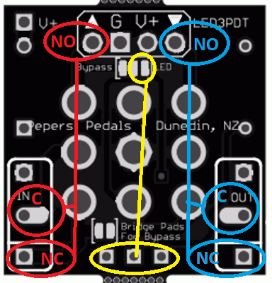
Setting it up for bypass is easy. Just chuck a big blob of solder on the two pads circled in the picture below. The bottom pad joins poles A and B together for the bypass part of the bypass. The top pads join the bypassed input signal of the effect to ground. I do it this way to ground the effect when not in use. for the LED in the configuration use the two pads that are circled at the top right of the board. The CLR and a Power Protection Diode are also installed on the board
 |
| Setup for Bypass |
Setting up to use a switch is also very easy. Just don't bridge the pads. You can see in the picture below which pads the contacts of the switch end up on. This time and Dual colour LED can be hooked up to the three LED pads and indicate either switch state
 |
| Setup as DPDT with LED indication |
So with that one done and dusted I thought why stop there. There have been a few pedals around with these new LED ringed 3PDT switches. They have a built in LED ring that lights up. They look quite good. I haven't used them on any of my builds but a fellow builder has. I was designing PCBs for this guy and thought hey why not do some daughter boards that you can use with these switches. So I did.


So sticking with the same formula I drew up some more PCBs
 |
| In Gerber viewer |
Just like above they are setup the same. Bridge the pads for bypass with the exception of a 3 way pad to wire to the LED
With the PCBs all drawn up I then put as many as I could onto a 100mm x 100mm panel.
 |
| For bypass |
 |
| For use as a DPDT with Dual LED indication |
My method of panalizing is probably the slowest but it works for me. What I do is make a copy of the .BRD file into another folder which severes the connection between schematic and board. I then draw 1.016mm or 40mil line on the milling layer for a milling cut. I also made a custom part of a row of 7 0.5mm hole to make the mouse bites. Once I'm happy with the milling lines and mouse bites on one of the boards I select the whole lot and copy it, Then I paste a copy and line it up with the original. Rinse and repeat to fill a 100mm x 100mm panel. I process the board in the CAM processor and then have a look at the gerber file. Adjust anything that needs adjusted and reprocess. You'll notice in the below screen capture of the board there are a mix of PCBs. 10 x 3PDT 2 x Miniature 3PDT and 4 x LED ring 3PDT . I'm going to do a post on how I panalize at some stage in the future. The boards are currently in production at DirtyPCBS
 |
| Panalized board put into the Seeedstudio gerber veiwer |
For anyone that is interested here is a dropbox link to my switch library PP-Switches
Here is what they look like in EAGLE. The outline is in the "TEST" layer so they don't appear on your processed Gerber
Here is what they look like in EAGLE. The outline is in the "TEST" layer so they don't appear on your processed Gerber


boards look nice but shipping is a little rediculus!!! oh well
ReplyDeleteI could ship those boards,40 for about $3.75 or so
ReplyDelete